TPS61291DRVR

TEXAS INSTRUMENTS INC
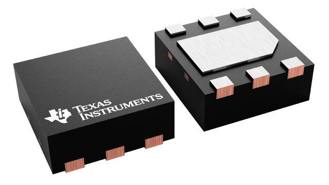
TPS61291DRVR
 
TPS61291DRVR

TPS61291DRVR

Availability
Constrained
Availability
Design risk
Low
Design risk
Price trend
Increasing
Price trend
Lead time
Stable
Lead time
15 results found
SGA6586Z
Available
Available
High
High
Stable
Stable
Stable
Stable
74HC4053BQ
Constrained
Constrained
Medium
Medium
Stable
Stable
Stable
Stable
CR16-512-JY
Available
Available
High
High
Stable
Stable
Stable
Stable
MAX845ESA+T
Available
Available
Medium
Medium
Decreasing
Decreasing
Stable
Stable
95157-210VLF
Constrained
Constrained
Low
Low
Decreasing
Decreasing
Stable
Stable
CR32-3000-FL
Unavailable
Unavailable
Low
Low
Stable
Stable
Stable
Stable
SS10U100PQF1
Available
Available
High
High
Stable
Stable
Stable
Stable
WR04X3001FTL
Unavailable
Unavailable
Low
Low
Decreasing
Decreasing
Decreasing
Decreasing
115A-BDA0-R01
Available
Available
High
High
Decreasing
Decreasing
Stable
Stable
ADM3222ARUZ-REE...
Constrained
Constrained
Low
Low
Stable
Stable
Decreasing
Decreasing
TCJ5477M016R010...
Available
Available
High
High
Decreasing
Decreasing
Stable
Stable
293D105X9035A2T...
Constrained
Constrained
Low
Low
Stable
Stable
Stable
Stable
MX29LV640ETTI-7...
Constrained
Constrained
Low
Low
Decreasing
Decreasing
Increasing
Increasing
DFE201610P-1R0M...
Unavailable
Unavailable
Low
Low
Stable
Stable
Increasing
Increasing
DFE252012F-1R0M...
Unavailable
Unavailable
Low
Low
Stable
Stable
Increasing
Increasing

Semiconductors

Other Semiconductors

Lead Time     18 weeks
Data Sheet     Download TPS61291DRVR datasheet TPS61291DRVR

Low Iq Boost Converter with 15nA Bypass Operation 6-WSON -40 to 125

Technical Data

Manufacturer texas instruments inc
MPN TPS61291DRVR
Width (mm) 2.0000
Length (mm) 2.0000
Control Mode CURRENT-MODE
JESD-30 Code S-PDSO-N6
Package Code HVSON
Package Shape SQUARE
Package Style ( Meter ) SMALL OUTLINE, HEAT SINK/SLUG, VERY THIN PROFILE
Surface Mount YES
Terminal Form NO LEAD
J-STD-609 Code e4
Terminal Finish Nickel/Palladium/Gold (Ni/Pd/Au)
Control Technique HYSTERETIC CURRENT MODE
Number of Outputs 1.0000
Temperature Grade INDUSTRIAL
Terminal Position DUAL
Additional Feature ALSO AVAILABLE IN 3, 3.3V OUTPUT
Number of Functions 1.0000
Number of Terminals 6.0000
Terminal Pitch (mm) 0.6500
Input Voltage-Max (V) 5.0000
Input Voltage-Min (V) 0.9000
Input Voltage-Nom (V) 1.2000
Package Body Material PLASTIC/EPOXY
Analog IC - Other Type SWITCHING REGULATOR
Output Current-Max (A) 1.3000
Output Voltage-Max (V) 3.3000
Output Voltage-Min (V) 2.5000
Output Voltage-Nom (V) 2.5000
Seated Height-Max (mm) 0.8000
Switcher Configuration BOOST
Moisture Sensitivity Level 2.0000
Peak Reflow Temperature (Cel) 260.0000
Switching Frequency-Max (kHz) 2300.0000
Operating Temperature-Max (Cel) 85.0000
Operating Temperature-Min (Cel) -40.0000
Time@Peak Reflow Temperature-Max (s) 30.0000
Availability In stock

Submit Request

CONTACT REASON

Connect With Us

HEADQUARTERS

Sourceability North America, LLC

9715 Burnet Rd, Ste 200 Austin, TX 78758-5215

Frequently Asked Questions

As part of the category Semiconductors and subcategory Other Semiconductors, TPS61291DRVR optimizes energy distribution in electronic devices. Its Low Iq Boost Converter with 15nA Bypass Operation 6-WSON -40 to 125 allows minimizing losses and increasing the overall system efficiency.

As a component of the subcategory Other Semiconductors, TPS61291DRVR ensures stable output voltage even when the load changes. Its makes it a reliable element in multi-level power systems.

You can download the user manual and technical specifications for TPS61291DRVR in the documentation section.

Low Iq Boost Converter with 15nA Bypass Operation 6-WSON -40 to 125