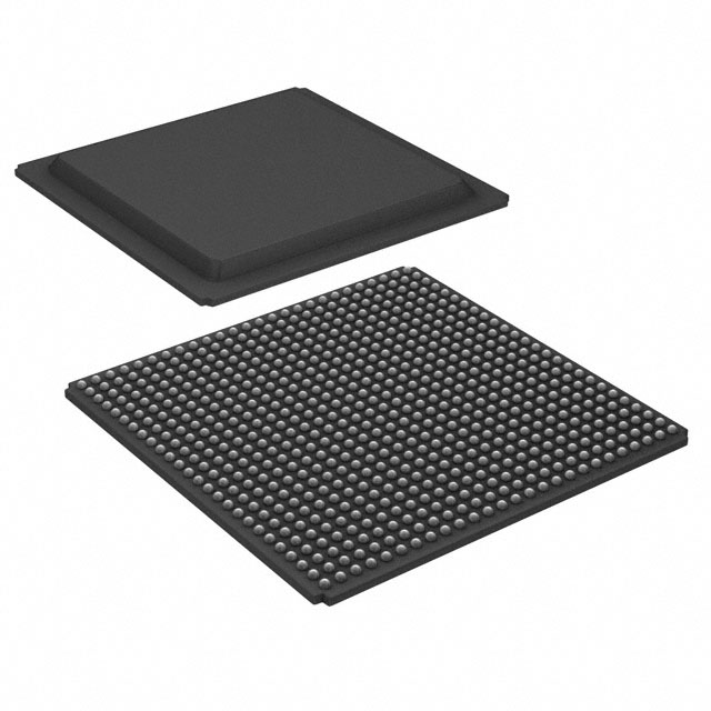
XC7A100T-2FGG676I
Availability
Design risk
Price trend
Lead time
IC FPGA 300 I/O 676FBGA
Technology | CMOS |
Width (mm) | 27 |
Length (mm) | 27 |
JESD-30 Code | S-PBGA-B676 |
Organization | 7925 CLBS |
Package Code | BGA |
Package Shape | SQUARE |
Package Style (Meter) | GRID ARRAY |
Surface Mount | YES |
Terminal Form | BALL |
J-STD-609 Code | e1 |
Number of CLBs | 7925 |
Terminal Finish | TIN SILVER COPPER |
Number of Inputs | 300 |
DLA Qualification | Not Qualified |
Number of Outputs | 300 |
Temperature Grade | INDUSTRIAL |
Terminal Position | BOTTOM |
Number of Terminals | 676 |
Terminal Pitch (mm) | 1 |
Number of Logic Cells | 101440 |
Package Body Material | PLASTIC/EPOXY |
Seated Height-Max (mm) | 2.44 |
Supply Voltage-Max (V) | 1.05 |
Supply Voltage-Min (V) | 0.95 |
Supply Voltage-Nom (V) | 1 |
Programmable Logic Type | FIELD PROGRAMMABLE GATE ARRAY |
Package Equivalence Code | BGA676,26X26,40 |
Clock Frequency-Max (MHz) | 1286 |
Moisture Sensitivity Level | 3 |
Peak Reflow Temperature (Cel) | 250 |
Operating Temperature-Max (Cel) | 100 |
Operating Temperature-Min (Cel) | -40 |
Time@Peak Reflow Temperature-Max (s) | 30 |
Combinatorial Delay of a CLB-Max (ns) | 1.05 |
Submit request
CONTACT REASON
Sourceability North America, LLC
9715 Burnet Rd, Ste 200You can download the user manual and technical specifications for Advanced Micro Devices, Inc. (AMD) XC7A100T-2FGG676I in the documentation section.
IC FPGA 300 I/O 676FBGA
As part of the category Semiconductors and subcategory Semiconductors, XC7A100T-2FGG676I optimizes energy distribution in electronic devices. Its IC FPGA 300 I/O 676FBGA allows minimizing losses and increasing the overall system efficiency.
As a component of the subcategory Semiconductors, XC7A100T-2FGG676I ensures stable output voltage even when the load changes. Its IC FPGA 300 I/O 676FBGA makes it a reliable element in multi-level power systems.