NT6AN512T32AV-J2

NANYA TECHNOLOGY CORP
no image
 
NT6AN512T32AV-J2

NT6AN512T32AV-J2

Availability
Available
Availability
Design risk
High
Design risk
Price trend
Stable
Price trend
Lead time
Stable
Lead time

15 results found
TPS25221DRVR
Constrained
Constrained
Low
Low
Increasing
Increasing
Stable
Stable
PESD2IVN24-TR
Constrained
Constrained
Low
Low
Stable
Stable
Increasing
Increasing
0402B102K500CT
Constrained
Constrained
Low
Low
Stable
Stable
Stable
Stable
0402B103K160CT
Constrained
Constrained
Low
Low
Stable
Stable
Stable
Stable
0603B334K160CT
Constrained
Constrained
Low
Low
Decreasing
Decreasing
Decreasing
Decreasing
ADS7138QRTERQ1
Constrained
Constrained
Low
Low
Stable
Stable
Stable
Stable
DF9-31S-1V(32)
Constrained
Constrained
Low
Low
Stable
Stable
Decreasing
Decreasing
DLP31DN131ML4L
Available
Available
High
High
Decreasing
Decreasing
Decreasing
Decreasing
APW8707BQBI-TRG
Available
Available
High
High
Stable
Stable
Stable
Stable
CL10A106MQ8NNNC
Unavailable
Unavailable
Low
Low
Decreasing
Decreasing
Increasing
Increasing
RK73H1JTTD93R1F
Unavailable
Unavailable
Low
Low
Decreasing
Decreasing
Stable
Stable
X1A000121000500
Available
Available
High
High
Decreasing
Decreasing
Stable
Stable
S25FL064LABMFI0...
Unavailable
Unavailable
Low
Low
Decreasing
Decreasing
Stable
Stable
S29GL256S90TFI0...
Unavailable
Unavailable
Low
Low
Stable
Stable
Stable
Stable
XC6SLX100-2FGG4...
Available
Available
High
High
Stable
Stable
Stable
Stable

Semiconductors

DRAMs

Lead Time     8 weeks
Data Sheet     Download NT6AN512T32AV-J2 datasheet NT6AN512T32AV-J2

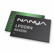
DRAM Chip Mobile LPDDR4 SDRAM 16Gbit 512Mx32 1.1V/1.8V 200-Pin FBGA

Technical Data

Manufacturer nanya technology corp
MPN NT6AN512T32AV-J2
I/O Type COMMON
Technology CMOS
Width (mm) 10.0000
Access Mode MULTI BANK PAGE BURST
Length (mm) 15.0000
JESD-30 Code R-PBGA-B200
Memory Width 32.0000
Package Code VFBGA
Self Refresh YES
Package Shape RECTANGULAR
Package Style ( Meter ) GRID ARRAY, VERY THIN PROFILE, FINE PITCH
Surface Mount YES
Terminal Form BALL
Memory IC Type LPDDR4 DRAM
Operating Mode SYNCHRONOUS
Refresh Cycles 8192.0000
Number of Ports 1.0000
Temperature Grade OTHER
Terminal Position BOTTOM
Additional Feature AUTO/SELF REFRESH; IT ALSO REQUIRES 1.8V NOMIMAL SUPPLY VOLTAGE; TERM PITCH-MAX
Memory Organization 512MX32
Number of Functions 1.0000
Number of Terminals 200.0000
Terminal Pitch (mm) 0.8000
Number of Words Code 512M
Memory Density (bits) 17179869184.0000
Package Body Material PLASTIC/EPOXY
Output Characteristics 3-STATE
Seated Height-Max (mm) 1.0000
Supply Voltage-Max (V) 1.1700
Supply Voltage-Min (V) 1.0600
Supply Voltage-Nom (V) 1.1000
Number of Words (words) 536870912.0000
Sequential Burst Length 16,32
Standby Current-Max (A) 0.0600
Supply Current-Max (mA) 680.0000
Interleaved Burst Length 16,32
Package Equivalence Code BGA200,12X22,32/25
Clock Frequency-Max (MHz) 1866.0000
Peak Reflow Temperature (Cel) NOT SPECIFIED
Operating Temperature-Max (Cel) 105.0000
Operating Temperature-Min (Cel) -30.0000
Time@Peak Reflow Temperature-Max (s) NOT SPECIFIED
Availability In stock

Submit Request

CONTACT REASON

Connect With Us

HEADQUARTERS

Sourceability North America, LLC

9715 Burnet Rd, Ste 200 Austin, TX 78758-5215

Frequently Asked Questions

As part of the category Semiconductors and subcategory DRAMs, NT6AN512T32AV-J2 optimizes energy distribution in electronic devices. Its DRAM Chip Mobile LPDDR4 SDRAM 16Gbit 512Mx32 1.1V/1.8V 200-Pin FBGA allows minimizing losses and increasing the overall system efficiency.

As a component of the subcategory DRAMs, NT6AN512T32AV-J2 ensures stable output voltage even when the load changes. Its makes it a reliable element in multi-level power systems.

You can download the user manual and technical specifications for NT6AN512T32AV-J2 in the documentation section.

DRAM Chip Mobile LPDDR4 SDRAM 16Gbit 512Mx32 1.1V/1.8V 200-Pin FBGA